Final Project Update

The status of the project is complete.We implemented layer one and layer two in hardware, and we left layer three and layer four in software. Our initial design proved to be a good design. Upon implementing layer two in hardware, we started optimizing the system by changing the weights and the biases. We came up with a clever data compression algorithm to reduce the amounts of bits required for storing the biases, the weights, and the inputs in memory that did not cause a huge loss of accuracy. We exploited parallelism to read as many weights, biases, and pixel inputs at a time.

As of the final submission, we were able to achieve a 98% reduction in run-time, resulting in a time of 5.55 ms per sample, with an overall accuracy of 96%.

We achieved a speed up of 62X

There is definitely huge room for improvement, but we choose to stop at 5.44 ms, because obviously of time constraints. If given the time, this system can be optimized to have a runtime of less than 0.016 ms, and it is not hard to get such reduction in run-time, but it just requires time.

Update 2: Optimization Phase

Right after the first milestone—after having implemented layers one in hardware—we started optimizing the system. We value accuracy, so in our optimization we made changes that caused the least amount of reduction in accuracy. We came up with a compression method for compressing the weights, inputs, and the biases where we use less bits,but still retain only 1% loss in accuracy.

A few weeks ago, after implementing layer two in hardware, we were able to achieve a time of 54.004400 ms per sample, with an accuracy of 96.61%. The picture below shows this in more details.

We reduced the number of bits used to store the weights, the biases and the inputs, and we were able to achieving a run-time of 34.588 ms per sample, with an accuracy of 96.61. See the picture below for more details:


Milestone 1: Working Hardware-Software Demo

Today, we demonstrated to the TA the functionality of our system. At this point, we were able to implement layer2 in hardware. Having only layer2 implemented using hardware results in a time of 80ms per sample image. This is an improvement from the 352ms. This is still above the cutoff time. Next, we are going to implement layer3 in hardware. With layer3 implemented in hardware, we should be able to achieve at most 10 ms per sample. Overall, the initial design seems to be working fine. Here’s a picture of the output times and accuracy per cent of the current system.

layer2_HW_implementation_results

Update 1: Design Plan Presentation

Our design plan presenation was on April 17, 2017. Before the presentation day, we conducted a lot of analysis.  We used Gprof in Linux to do a runtime profiling of our implementation of the Neural networks algorithm. We found that layers2 and 3 to be the most costly in terms of time. These two layers accounted for nearly 99% of all computational time. The picture below shows the results from running Gprof.

Having known this information, we created a very good design that implements layers 2 and 3 on the FPGA. On the FPGA we would exploit parallelism and would pipeline the system in order to achieve large speed ups. Here’s the algorithm flow chart:

algorithm diagram

The Algorithm follows the flowchart is outlined as follows:

  1. In software, read the weights, the biases, and the inputs from the SD Card and save them in SDRAM.
    1. The data is written in SDRAM in the same order we plan to access it.
    2. The input test data is rounded and can be saved as a single bit.
  2. Start the timer.
  3. Send start signal to hardware using a PIO.
  4. Read all 784 inputs from SDRAM and save them in registers on the FPGA.
  5. Read the first column of weights from SDRAM and save in FPGA registers.
  6. In parallel, AND the input data (200×1 matrix) and the column of weights (200×1 matrix). This results in another 200×1 matrix that is saved in 200 FPGA registers, referred to as the ‘result’ registers.
  7. Load the next column (200 reads) of weights and save them in the same registers as used before.
  8. In parallel, AND the input data and the column of weight. Add the result with what is currently stored in the ‘result’ registers.
  9. Repeat steps 6 and 7 for all 784 columns in the weight matrix.
  10. Read 200 biases from SDRAM and save them in registers on the FPGA.
  11. In parallel, add 200 biases to the data in the 200 result registers.
  12. Take the sigmoid of the data stored in the 200 result registers and save the result in the same registers.
  13. Repeat the same process described above with the following changes.
    1. Use the result registers as the input.
    2. Use the weights for layer 3.
    3. Instead of ‘ANDing’ the inputs and weights, they must be multiplied.
    4. Steps 6 and 7 only need to be repeated 200 times since the weight matrix for layer 3 is 200×200.
  14. Write the resulting 200×1 matrix to SDRAM.
  15. Send done signal to software using a PIO.
  16. In software, multiply the weights for layer 4 and take the sigmoid to get a 10×1 matrix.
  17. Find and output the index of the greatest number in the matrix and output.

Here’s the RTL Diagrams for the design:

RTL1

RTL2

We calculated the time required one sample by calculating the time needed to perform the software part, and the time needed to perform the hardware part. For the software part, we used Gprofile, to get precise measurements. For the hardware part, we calculated the precise estimate of number of clock cycles needed to perform the computation, and calculated the actual time estimate from the given 50 MHz clock frequency. We found that such implementation would result in a 43X speed up.


LAB 5: HAND WRITTEN DIGIT RECOGNITION AND CLASSIFICATION ALGORITHM

In this lab, we developed an image processing algorithm to detect and recognize handwritten digits. The main goal of the lab was to familiarize ourselves with neural networks. Neural networks are a class of machine learning algorithm where individual units are connected via weights and those weights are adjusted as the network is trained. An example of a neural network is shown below.

In this lab, we were given a specific neural network that has already been trained to predict handwritten digits with an accuracy of 97%. The network in figure 1 was given, and it has 784 input nodes which each correspond to one pixel of an input image. The complete specifications of the network are given in details in the lab manual.

In the first part we learned how to set up the ANN in MATLAB and classify any given picture of a hand-written digit. Also, we wrote simple MATLAB function that can fetch and display a certain image from our test dataset. This function was useful to debug the code and to visually double check the prediction of our algorithm. The overall accuracy of our MATLAB implementation is 97.91%.We take note of the time, and it took a long time.

After we understood how ANN works and implemented it in MATLAB, we made a C implementation of the MATLAB code. Basically, we started with an implementation that can run on any Linux machine. Then we moved our code to the DE1-Soc Linux system and made the weights and test data files get loaded directly from the SD CARD to SDRAM. The classification accuracy dropped a little bit to 97.4%. Probably that slight change was due to changing the way we represent the test data. Basically, when we saved the test data from MATLAB we rounded it first to the nearest integer value (0 or 1). That represents converting the test image from a greyscale image to back and white image. That conversion allowed us to represent each pixel as one byte of data (uint8) instead of a double precision floating points. Hence, out test data file become much smaller and we were able to load it to memory faster. We then set up the neural network in C and ran the neural network on the HPS, and took note of the computation time. It took more than 350ms per sample image.

While performing this lab, we encountered several problems. One of the problems we had was storing the weights into the SDRAM. The given weights are all very small numbers with powers of 10^(-6), and storing them on the SDRAM proved no easy task. To read the weights, we used the function `fread()` in C from a file. Another problem was figuring out how the Matlab function stored the greyscaled matrix. There two possible ways: column major order and row major order. We found out that the Matlab function `fwrite()` uses column major order to store the matrix. After knowing this information, storing the weights and running the neural network became easy.

USEFUL RESOURCES:
Neural Networks Demystified (Video) <—- the best resource

Introduction to Artificial Neural Networks(pdf)

Hacker’s Guide to Neural Networks(web)

A Basic Introduction To Neural Networks

Introduction to Deep Neural Networks

Machine Learning is Fun


Lab4: Running Linux On DE1—SOC Board

In the first part of this lab, we learned how to configure the board’s HPS to run a modified version of the Linux Operating System. We downloaded the modified Linux OS from Terasic’s Website. We then burned the OS to an SD card, and connected the keyboard & mouse and a monitor using the VGA port, and booted the Linux OS.

Although we followed the lab manual step by step, we were unable to get Linux running on the HPS from the first try. We had to change the QSYS system many times, do a lot of modifications until we were able to run Linux on the HPS. Most of the problems came from the QSYS system. Other than QSYS, we noticed that the VGA port is very unstable, and small movements around the wire can cause it to blink.

The second part of the lab was to implement edge detection on a given image (particularly lenna.jpg). The image is 512×512 pixels. First, we use Matlab to convert the image to greyscale and use 8-bits per pixel. We saved the values of the converted picture as a two-dimensional array in a text file. Using Matlab, we coded Sobel’s algorithm and found the edges of the picture. After having completed the edge detection in Matlab, we moved on implementing the algorithm in C on the HPS.

     Before Edge Detect             After Edge Detection

On the HPS, we read the pixels of the image, and stored them on the FPGA’s SDRAM. We then read the values from the FPGA SDRAM and stored them into a 512×512 matrix on the HPS on-Chip. We implemented Sobel’s algorithm in C, and ran the algorithm with the given image, and  stored the values back into a matrix of size 512×512 into the FPGA SDRAM. We checked the result matrix with the matrix from Matlab and verified that the C algorithm worked correctly. We then moved on accelerating the algorithm using Verilog.

We started by using the FPGA to accelerate the computations by doing many computations in parallel. Instead of reading one pixel at a time, we read 3 rows of 4 pixels at a time, and then the calculation took only one clock cycle. At the same time more pixels were created.  We started with basic accelerations, and had planned on dividing  the work and adding pipelining, but were unable to implement such advanced optimization methods due to limited time.

USEFUL RESOURCES:

Running Linux on DE1-SoC Board Tutorial(pdf)

Running Linux on DE1-SoC Board Video

DE1-SoC Reference Book

Lenna, The First Lady of the Internet  (<—- Lenna the story behind the picture)


LAB 3: DESIGNING AVALON MEMORY MAPPED MASTER COMPONENTS

This lab was a very long lab. We learned how to design an Avalon Memory Mapped Slave component capable of controlling multiple slaves. Some of the signals were similar to what we used to lab2 while designing the slave component. However, this time we learned how to make a Verilog module that acts a master component and that drives those signals. The signals for the master component are shown below:

We faced a lot of challenges while doing this lab. In the first part we had two approaches to make our master component read and write to the 32-bit register. The first was to create a state machine that defines a state for the system at any given point in time depending on the inputs to the systems and the previous state. This approach didn’t work out well because of synchronization issues. We tried different strategies to get our state machine to work but we were not successful. That’s why we resorted to the second approach which is using different If statements (multiplexers) to define the output signals at any given point with respect to a global counter that we used to know when a second has passed. Sine one seconds of time is signified by 50 million counts, our system used very expensive comparisons to decide what to do next. Maybe that’s not the best approach to design our master component, but it worked and gave us the requires output.

In the second part of this lab, we faced multiple issues while we are trying to write and read to the SDRAM from our C code through Altera Monitor Program and our Verilog module. While writing the C code that stores ten numbers to ten different positions in the SDRAM we weren’t aware that each address in our SDRAM address space represents a 16-bit storage unit. In other words, thinking that our address represents a 32-bit words made us use Integers data types in C while dereferencing the pointer which contains the address. That made the compiler to translate each of our writing operation into writing to two consecutive SDRAM words. After we fixed that problem and made sure that our c code writes 16-bit words to each address, we tried to make our SDRAM master component read these values and deciding which is the maximum and the minimum values.  In order to give our Verilog module a start signal to read the 10 addresses initially we tried to use a sentinel value that’s being written to the 11th address by our C code. It turns out that’s not a good practice because when we power up our system our memory might have random values stored in it and there’s a chance that the 11th address already have our sentinel value. We learned afterwards that the best way to have a start and a finish trigger to our Verilog module is through Qsys PIO components.

The biggest stumbling block in this lab was getting our Verilog module to read the 10 addresses from the SDRAM. We tried designing different state machines that might had the right flow of logic; however, our implementation didn’t work. We managed to get our state machine to write data to a certain address in the SDRAM. Nevertheless, we were never able to read all the 10 addresses then move to the write state. For some reason our state machine implementation always gets stuck at some state and we didn’t have the proper tool to debug it. Later we learned about the SignalTap Logic Analyzer tool which enables us to look at the control signals on real time execution of our code on the board. Due to time constraints we were not able to debug our state machine and get it to work on time.

Useful Resources for this lab:

Altera Using SDRAM on DE1-SoC (pdf)

Altera Tutorial on Using SDRAM on DE1-SoC (pdf)

Helpful Question on SDRAM (stackoverflow)


LAB 2: CUSTOM QSYS COMPONENTS, USER I/O, FPGA AND HPS SDRAM MEMORY

In this lab we learned how to create a custom FPGA embedded component using Altera’s Qsys tool. We also learned how to interface the component with the HPS processor as an Avalon Memory-Mapped Slave. In the second part of the lab, we learned how to use the different types of memories available. We learned how to use SDRAM, DDR3 on the FPGA, and the DDR3 on the HPS system.

First we followed through the steps and created a 32-bit register module using Verilog. We simulated the module using ModelSim and ensured that it behaved as expected. We had a few logical problems, but we were able to fix them easily. Afterwards, on Qsys, we created a new component and instantiated the component in the Qsys system. On the Hard Processor System (HPS), we wrote a c-code to store and retrieve values into the register. We created a program that prompts the user to enter a 32-bit integer, which then the program displays on the six Seven-Segment-Displays and the LEDs. The program would keep asking the user to enter a new number until the user quits the program.

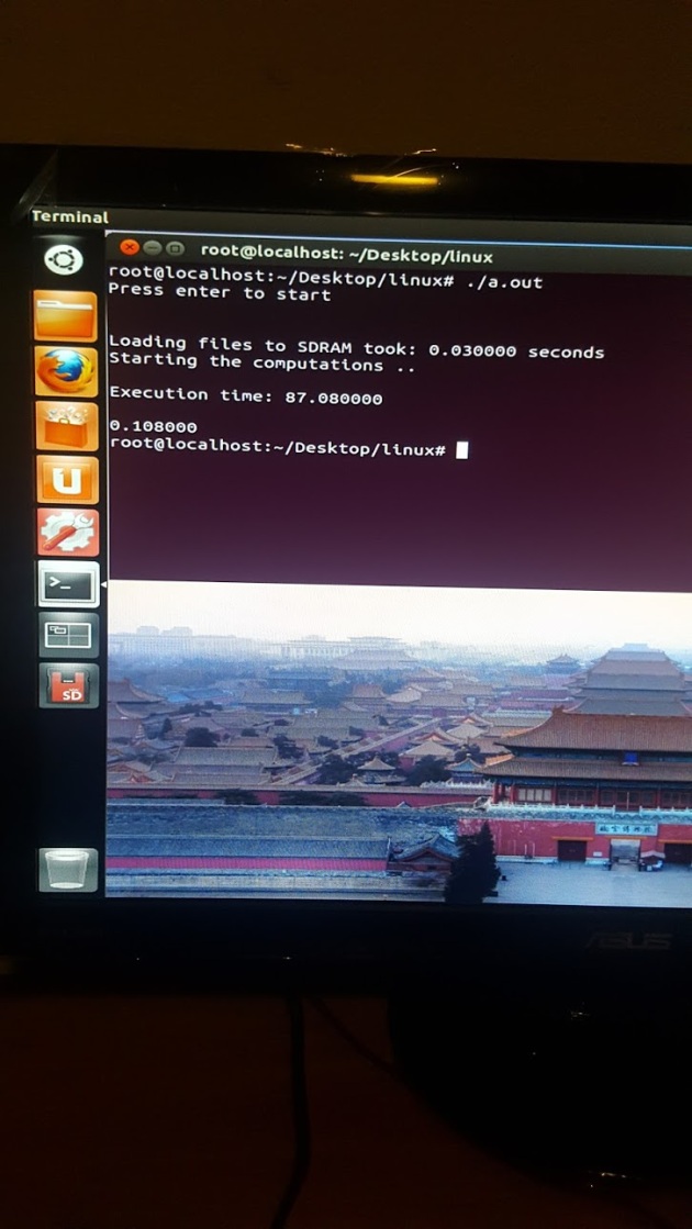
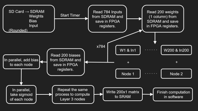
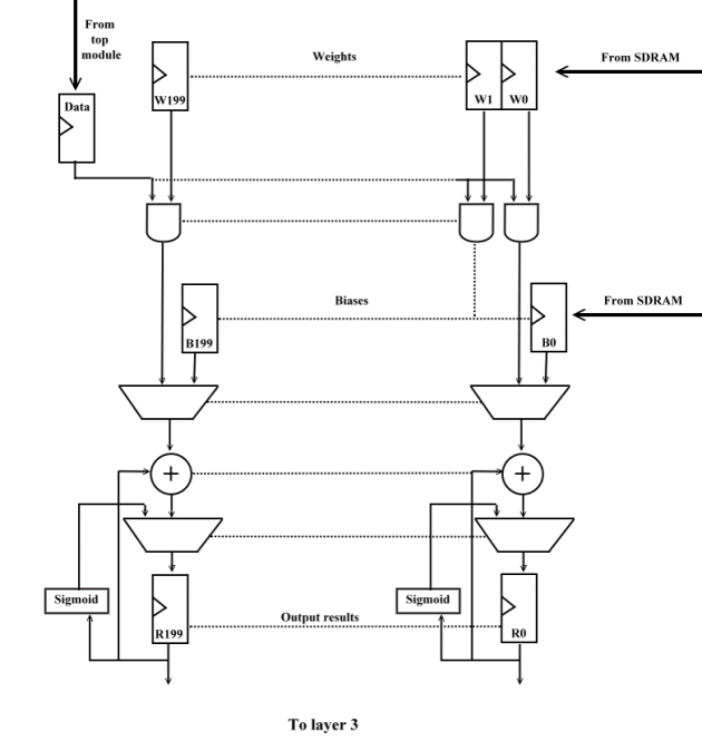
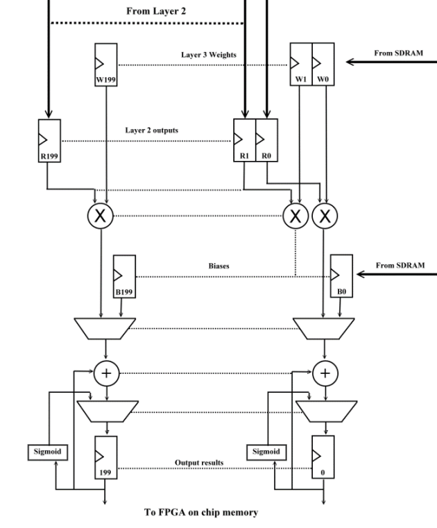
In the second part, we instantiated an SDRAM Controller in Qsys and integrating the component with our system. We instantiated the required components needed for communicating with SDRAM, the on-chip memory on the FPGA, and the on-chip memory on the HPS system. We took notes of the base addresses of the components and their respective busses’ address. We wrote C-code that ran on the HPS, which asked the user to choose one of the available rams to write and read data to. The available options were the On-Chip Memory on the FPGA, the FPGA SDRAM, the On-Chip memory of the HPS, and the HPS SDRAM (DDR3). Each time, we wrote 32KB of data into the selected memory and then read the data from the memory to verify that data was written correctly.

In the last part of the lab (Programming Assignment), we used everything we learned from previous parts of the lab to create a custom Verilog component that controlled the scrolling feature from lab1. We created a separate Verilog module, which takes inputs and bases on those inputs determines the required speed of the scrolling. This part was the most time consuming and we were not able to finish this part 100%. We came up with a state machine, and then we modeled the state machine using Verilog, and afterwards we debugged the state machine. Debugging the state machine was very tedious and required a lot of time. Every time we made a small change in the state machine, we had regenerate the Qsys system, and recompile. The compilation, on average, took 12 minutes to complete.  Even though we did not finish completely, we learned a lot about debugging Qsys systems from this part.

Useful Resources For this lab:

Offical Altera Tutorial on Creating Qsys Component (pdf)

Altera Tutorial on Creating Qsys Component Video (YouTube)

Altera handbook Creating Qsys Component (web)


LAB 1: DE1-SOC System Development Tutorial and Exercises

In this lab we learned about a special tools in Quartus II called Qsys, which is used to design digital systems. We used Qsys to design a hard processor system. In addition, we learned to control different peripherals on the board by using the built in Arm Cortex processor.

We gained experience reading and writing to the different board peripherals. We read values of the switches, and we sent values to the LED’s and programmed the six available 7-segment hex displays to scroll the phrase “Hello UUOrLD”. We also  learned how to display custom patterns on the 7-segment hex displays.

During this lab, we encountered a few problems. One of the problems that I personally encountered involved Quartus II software. Since I like getting a head start with labs, I downloaded and installed the licensed version of Quartus II, and when asked for the license, I provided the given license link in the lab to the UC Davis domain, and supposedly Quartus II accepted the license. However, when I started going through the tutorial lab, none of IP signals would show for the Hard Processor. I tried contacting Altera Support, but was turned down, because they only provide support through a ticket system, which takes a long time.

The solution to this problem was very trivial. I uninstalled the licensed version, and installed the free Web version. The free web version had all the signals, and supported the device family of the DE1-SOC Board.

We encountered other small problems using Pin Assignment tool, but their main cause was lack of following the lab manual thoroughly. In one of the steps, we accidentally skipped over, and so every time we used pin assignment, Quartus crashed. Following all the steps in the lab manual resolved this problem.

Overall, this was a very informative tutorial-lab. We learned alot about digital systems, and we are excited about the upcoming labs.